Hello,
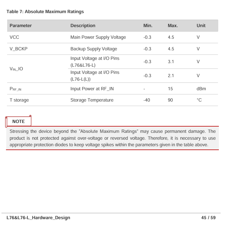
Reading the datasheets, it appears L86 and L76 GNSS modules have absolute limits for the signal IO pins specified as 3.1V:
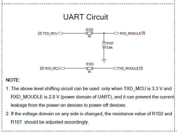
In an example circuit, it is suggested to use a voltage divider to interface 3.3V signaling to the 2.8V nominal input.
However, with a logic level UART, idle level signal is a high level, which results in current leakage through the resistor divider during idle time. This is a power waste for power-sensitive designs.
In a few places, I seem to see comments that suggest that 3.3V is an acceptable input signal level, despite the absolute limit specified in the datasheets.
The L76 EVB schematic, for example, connects the GNSS module to a USB transceiver or to a RS232 transceiver, both of which are expected to exceed Vih absolute limits.
What is the official recommendation/policy on this?