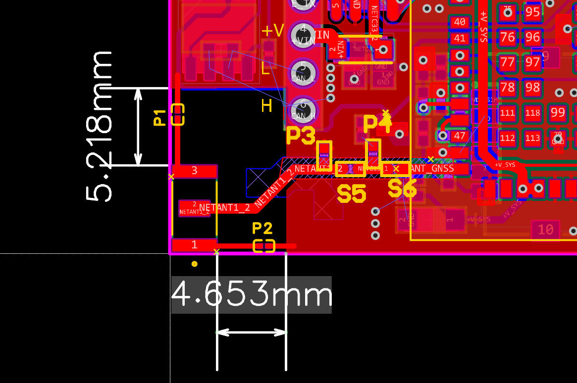
Hi, we use in our project GNSS antenna YCGS010AA, here is PCB layout of antenna placement.
What is the best way to position the antenna in this limited space? How critical is the change in the length of the tracks P1 and P2 from the recommended ones? Do I need to change the values of the capacitors in P1 and P2 or can I use the default? If so, what values of P1, P2, P3, P4, S5, S6 should I use?
P1, P2 track width 0.35mm
Transmission line width 0.7mm