Hello,
I am designing a PCB using a Quectel module L80-RE-37 and wanted to get some feedback on hardware design aspect. Though I have gone through the hardware design guidelines, I would like to get some feedback on the layout as some of the points mentioned in the document may not be followed.
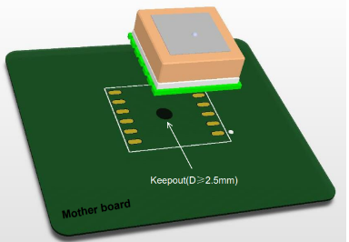
One thing is document has mention that there must be 5x5 mm keep out zone where no via, track, etc. are allowed. This may not be suitable to my design hence please confirm this.
rp354_jlc.zip (125.2 KB)
Hello @ujur007,
From what I can see on your PCB design, I can provide some guidelines.
Related to the keep out zone, If you are referring to feed point of patch antenna, the area should be more then 2.5mm in diameter and should be kept out on each layer.
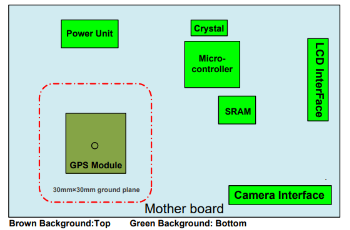
Make sure the microcontroller, crystal and other high-speed components and interfaces are placed on the opposite side of the module, as far as possible.
It would be very useful if you can provide values and names of the components or the schematic for your design.
Best Regards, Dobrica
Hello,
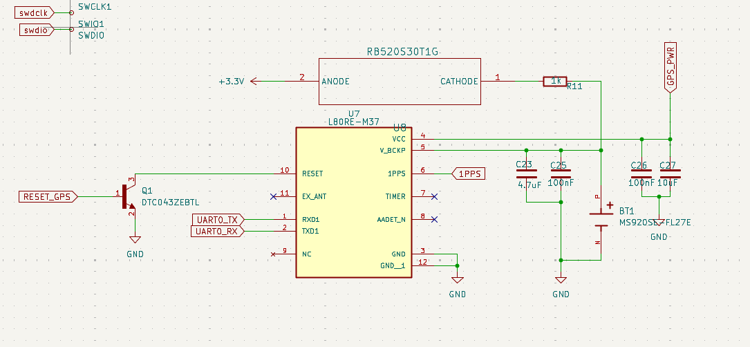
Here is a simplified schematic of the design, If you need full design, let me know, I can send you.
One question is what about the decoupling capacitors and other parts such as backup battery. Where these parts needs to be kept? Top later or bottom layer? They must be near to the module right?
Hi @ujur007,
Make sure that the capacitors with smaller value are closer to the module.
Regarding your question about placement, they should be placed in same layer as module itself.
Best Regards, Dobrica
Thank you, I will do the further steps. Let you know once the PCB is ready.