We have designed the BG96 to use a passive chip antenna SR4G008, but it is not working… there are conflicting instructions in the hardware design manual vs the reference design. Also the antenna manufacturer has suggested something different. We have originally designed it according to the antenna manufacturer. Please any assistance would be appreciated.
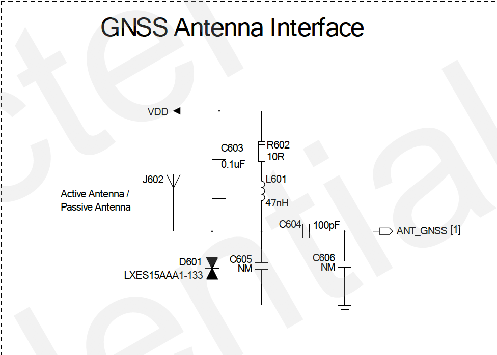
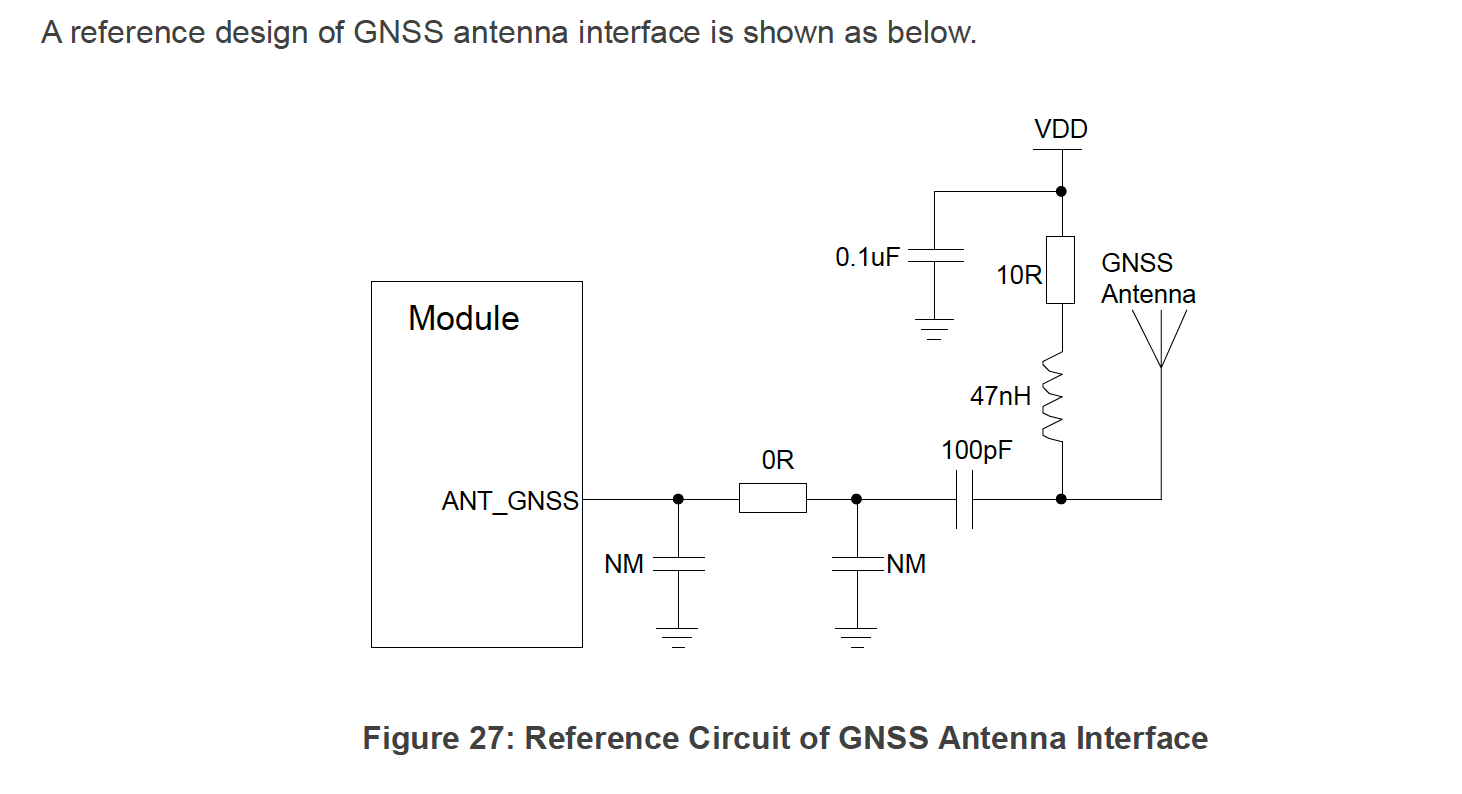
Below is the hardware design schematic vs the reference schematic vs the antenna manufacturer:
What do you mean by the conflict, the capacitance and resistance values of π type circuits? For specific values, please refer to the instruction manual of the attenna. The reference design of quectel is just a general reference,
I attached one quectel antenna design guide for you , pls kindly open the below comment
I mean conflict specifically the location and usage of the 100pf capacitor, in one design it is separate of the PI circuit, in the other it is a part of the PI circuit. I have followed the design guide of the antenna manufacturer which doesn’t include a 100pf capacitor but only a 1.5pf as I showed above, but it is not working that is why I am trying to figure out if I should have incorporated the 100pf into the PI circuit recommended by Quectel, or add it in addition to the PI circuit. That is the confusion.
Dear Stephen,
As mentioned in above schematic of BG96 reference design VDD of GNSS antenna
what should be the voltage of VDD ?
I have gone through complete hardware design documentation I haven’t found it.