Hi,
I’m going to use YG0062AA GNSS patch antenna for my project. I have a question about RF trace routing.
It can’t seem to route RF trace from the top side.
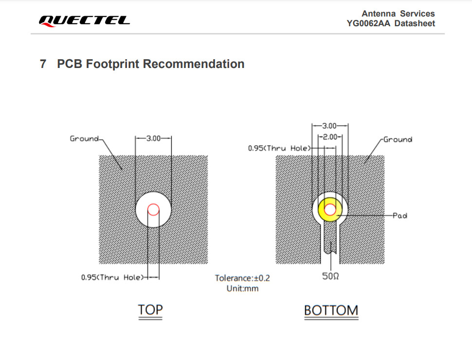
According to the datasheet, the top side of the TH pad is not plated and has a keep out area around it.
Does this mean I have to route the RF traces on the side opposite to the side the antenna is assembled on?
In other words, when the patch antenna is on the top side of the board, should the RF trace be routed on the bottom layer?
What do “TOP” and “BOTTOM” in above screenshot mean? Are they the top side and bottom side of the patch antenna? Or the top layer and bottom layer of PCB? I’m not sure of it.
If the patch antenna is assembled on the top layer of the board, is it possible to route RF trace on the top layer?
Looking forward to hearing from you soon.
Thanks in advance.
Milovan