LC29H BAMD stuck in strange state

I had designed an PCB that uses LC29H BAMD and LSCS were the ones who installed the components for me.

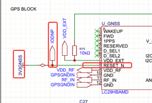
When I power on the module, the voltages of TX/RX, VCC, VDD_EXT, RESET_N, fluctuate quite wildly, and on the QGNSS serial monitor, I only see single byte outputs from the module. with all the fluctuating voltages, it really seems like the module is constantly rebooting.

If I tie REST_N to GND, the module Would also reset, but just resumes the single byte output.

the sole power source is from CH340C at 3v3.

Hi @Jason_Siu do you mind to share you PCB design? Besides, during the design did you refer to Quectel Hardware design guide? If no, please help to cross check your design using these documents:

  1. https://www.quectel.com/download/quectel_lc29h_series_reference_design_v1-4/
  2. https://www.quectel.com/download/quectel_lc29h_series_hardware_design_v1-4/

Best regards,

Hi Mr. Firdaus,

Thank you for your reply, my design mostly adheres to Quectel’s design requirements, but after looking at the documents you provided, I made some additional adjustments/bodges. The symptoms are rather different now. Previously, VDD_EXT would swing wildly, and the chip regularly prints the single byte count sentences as mentioned. Now VDD_EXT is very stable even after resets (RESET_N > GND) but serial monitor no longer sees any single byte count sentences.

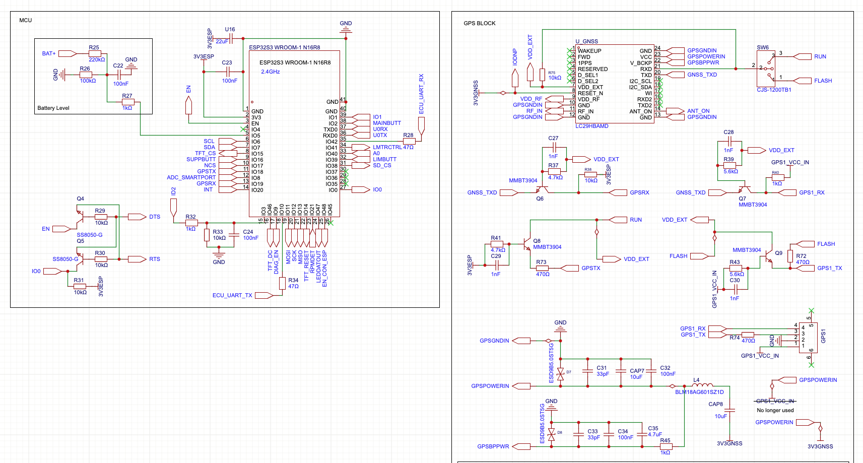
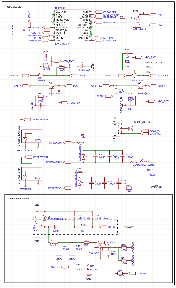
Also, since the board also has a ESP, I had added a circuit that switches flash and run state for the GNSS, please see schematics for your reference.

here are the voltages for the following pins with this design:
VDD_EXT - 2.74v stable
Pin 23 (GPSPOEWRIN) - 2.74v stable
pin 22 (GPSBPPWR) - 2.65v stable
pin 8 (RESET_N) - 2.69v stable

no activity in serial monitor

Hi @Jason_Siu below are my feedback:

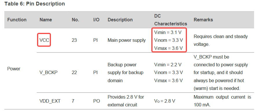
For you Pin23 (GPSPOWERIN) == VCC for LC29HBA is 2.74V was not enough. This has been mentioned in the Hardware design documentation as below:

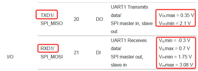
For RXD/TXD, please follow below DC characteristics:

Schematic review:

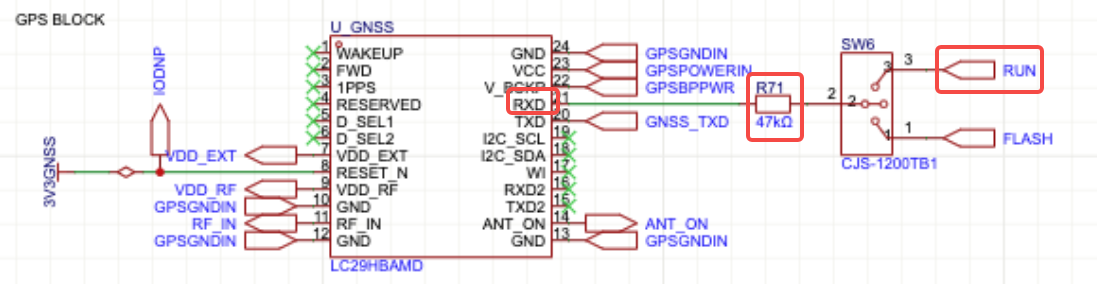
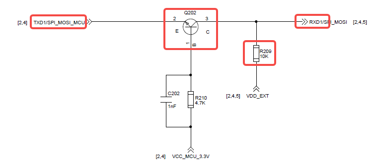
RXD Connectetion: RUN MODE

Reference design:


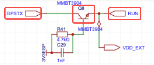
  1. Remove R71. Your Q8 MMBT3934 was in wrong direction. See reference design on the output arrow goes to MCU TXD (GPSTX).
  2. Additional 10K resistor similar to reference design R209 connected to VDD_EXT.

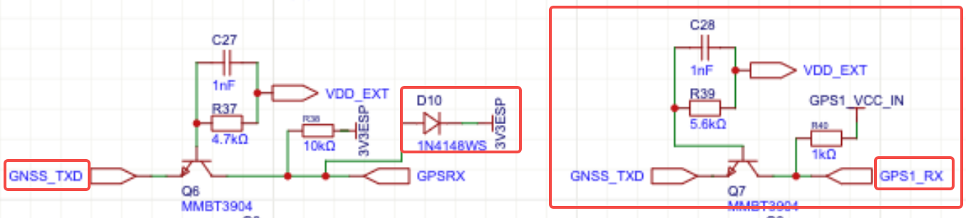
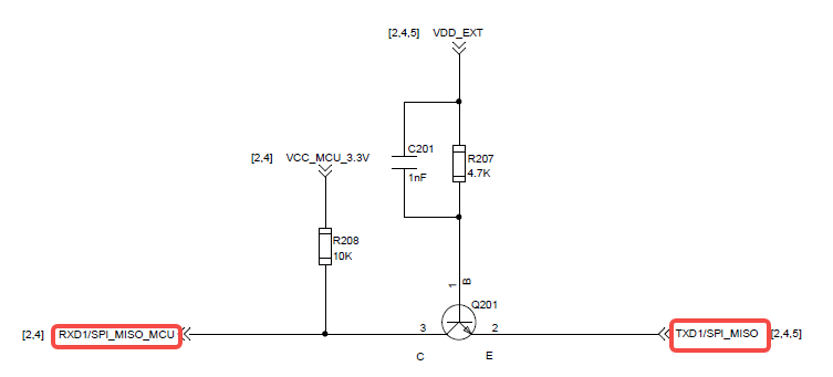
TXD Connection:

Reference design:


  1. May remove D10 if not needed.
  2. Why there are 2 GNSS_TXD connection to GPSRX and GPS1_RX?
  3. Keep follow the design similar to reference design.

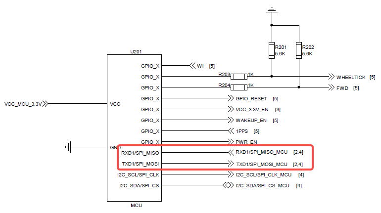
We were unable to complete a full review as the MCU connection could not be verified. Please thoroughly check your design against the reference design.

Best regards,

Dear Mr. Firdaus,

Thanks you for your comments, I’ve gone through all the changes:
Switched orientation for Q9 and Q8, taken out D10, taken our R71, added 10k resistor (reference R209)
And to make Q8 and Q9 work, I also removed the 2 BAT54 temporarily.

And now the VIN is measuring at 3.3, v_bkup is at 3.2v. however, pin 21 is at steady 2.8v, but pin 20 is also at steady 2.8v, not the 2.1v as stated in spec, if I reset_n, it will fluctuate briefly from 1.6, but it will end up sitting at 2.8v again. Also, Im still not getting any thing on the monitor either on QGNSS, tried all baud rates.

with regards to the 2 GNSS_TXD, the reason behind this design was that I left a 4 pin connector - GPS1, on the board so that I can flash firmware and send command directly to the LC29H, without the TXD lines from the MCU competing for the same lines. So both the GPS1 connector (which connects to an external CH340C for flashing) and the esp communicates with the LC29H. (I have attached schematics for your reference). and the SW6 is the physical toggle for switching between flashing the gnss (GPS1) and switching back to GNSS <> ESP communication.

Hi @Jason_Siu for Pin21 and Pin20, we are highly recommended to follow the DC characteristic based on the documentation. Can you help on below questions:

  1. How did try to get the NMEA output? Is it from ESP32 UART or from GNSS module directly?
  2. Can you try to get the output direct from GNSS module (by pass the ESP32)?
  3. Have you tried to re-flash the firmware?

Best regards,

Hello Mr. Firdaus,

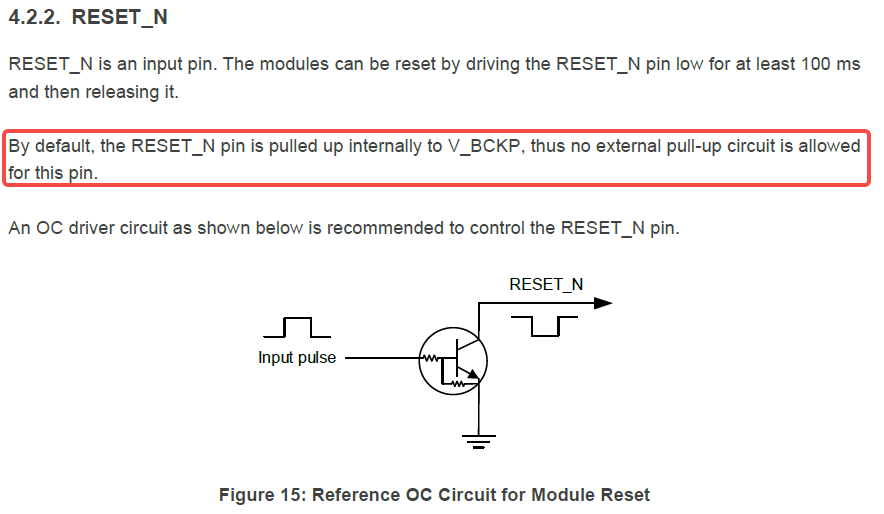
Thank you for the follow-up and for highlighting the DC characteristics for pins 20 and 21. We have adjusted our hardware toward your reference (Q8/Q9 orientation, 10 kΩ from VDD_EXT to module RXD1 / SW6-2, removal of the external RESET_N pull-up, and GNSS VCC at pin 23 ≥ 3.1 V after correcting our board power path). Below are direct answers to your three questions, then our remaining issue.


1. How did we try to get NMEA output — ESP32 UART or from the GNSS module directly?

We tried both, but not by probing pins 20/21 directly at the module.

  • ESP32 path (intended product use): UART1 on GPIO18/19 through our level shifters, with SW6 = RUN. For bring-up we often hold ESP in reset (EN low) so the ESP does not drive the bus.
  • CH340C path (bench / flash): The same adapter we have used successfully with LC29H breakout boards. On the KartHUD PCB we connect CH340 TX → GPS1 pin 2, CH340 RX → GPS1 pin 1, GND → GPS1 pin 3, 3.3 V I/O, 115200 8N1. SW6 = FLASH selects the dongle path through Q9. We do not apply CH340 VCC to GPS1 pin 4 for module power; the board supplies GNSS power. We added a bodge so Q9 base bias is fed from 3V3GNSS (pin 4 / GPS1_VCC_IN was too low when pin 4 was unused).

We have not seen NMEA on either path on this PCB. On a scope/DMM, TXD1 (pin 20) sits at about 2.81 V with no sustained UART activity; RXD1 (pin 21) is about 2.84 V at idle after the RX pull-up and shifter work.


2. Can we try output directly from the GNSS module (bypass the ESP32)?

Yes — that is our primary bench configuration. ESP traffic is disabled (EN held low or ESP not driving UART), SW6 = FLASH, and we use CH340 on the GPS1 header only as above. This bypasses the ESP32 while still going through our Q6/Q7 (TX out) and Q9 (RX in) circuits as per the integrated design — we are not wiring the CH340 straight to module pins 20/21.

We verified multiple CH340C adapters on breakout boards (same module, same tool versions); those adapters work for NMEA and flashing. On the KartHUD board, with the same adapters and module, we still get no UART data on GPS1 RX at 115200 (or other baud rates we tried).


3. Have we tried to re-flash the firmware?

Yes — that was one of the first steps. We use QGNSS with the same CH340C setup (SW6 = FLASH, GPS1 wiring as above).

The tool does not get past the “reset module” prompt. We have tried:

  • Pulling RESET_N (pin 8 / IODNP test pad) to GND for more than 100 ms, then releasing
  • A full power cycle (removing USB/battery so module VCC at pin 23 actually drops, not only ESP reset)

In all cases, QGNSS does not appear to detect a successful restart. We suspect this is related to there being no UART traffic from the module to begin with (nothing on GPS1 RX for the tool to synchronize with), but we would appreciate your confirmation of what the tool expects after reset (e.g. a specific boot message or baud).


DC characteristics (pins 20 & 21)

We are following the documented levels: idle TXD1 ~2.8 V (VDD_EXT domain), RXD1 biased via 10 kΩ to VDD_EXT, and host TX into the module through Q8/Q9 rather than 3.3 V direct on pin 21. We understand we must not “sag” TXD1; we are focusing on correct level shifting on the host side. We are still verifying with a scope that RXD1 reaches VIL/VIH when CH340 transmits.


Could you please advise on:

  1. For QGNSS, is a bootloader or banner on TXD1 after reset required for the tool to recognize that the module has restarted?
  2. With D_SEL1/D_SEL2 left floating (default UART mode on our PCB), is that sufficient for UART firmware upgrade, or is download-mode strapping on D_SEL also required for LC29H(BA)?
  3. If TXD1 is idle at ~2.8 V with no TX edges for an extended period after valid VCC and reset, but the same module still works on a breakout board, should we treat the issue as host PCB interface rather than a defective module?

Thank you again for your help.
Dear Mr. Firdaus,

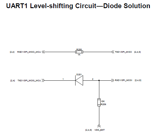
I have switched the schematics to just the diode + resistor configuration as opposed to using the npn network. the module is working perfectly now. I see sentence printouts.

But one lingering issue still remains, when I reset the module, I now see relevant messages printed in the serial monitor to indicate that the module has indeed rebooted. but the firmware upload tool still§ does not recognize the reset event. Despite trying various combinations of presses, the flashing tool just eventually times out by itself.

the reason why I need to flash the firmware is that I find most settings only stick or are recognized by the module only on a fresh firmware, especially when it comes to setting baud rate. I need the module to be at 921600 but it’s now stuck at 115200. RESTOREPAR*13 doesnt seem to work to restore the settings to factory default for the chip.

Are there other more reliable commands or methods where I would not need to flash the firmware to restore to factory default?

Hi @Jason_Siu Good to know that it is working now! To restore to default configuration, yes, you will need to use the $PQTMRESTOREPAR command.

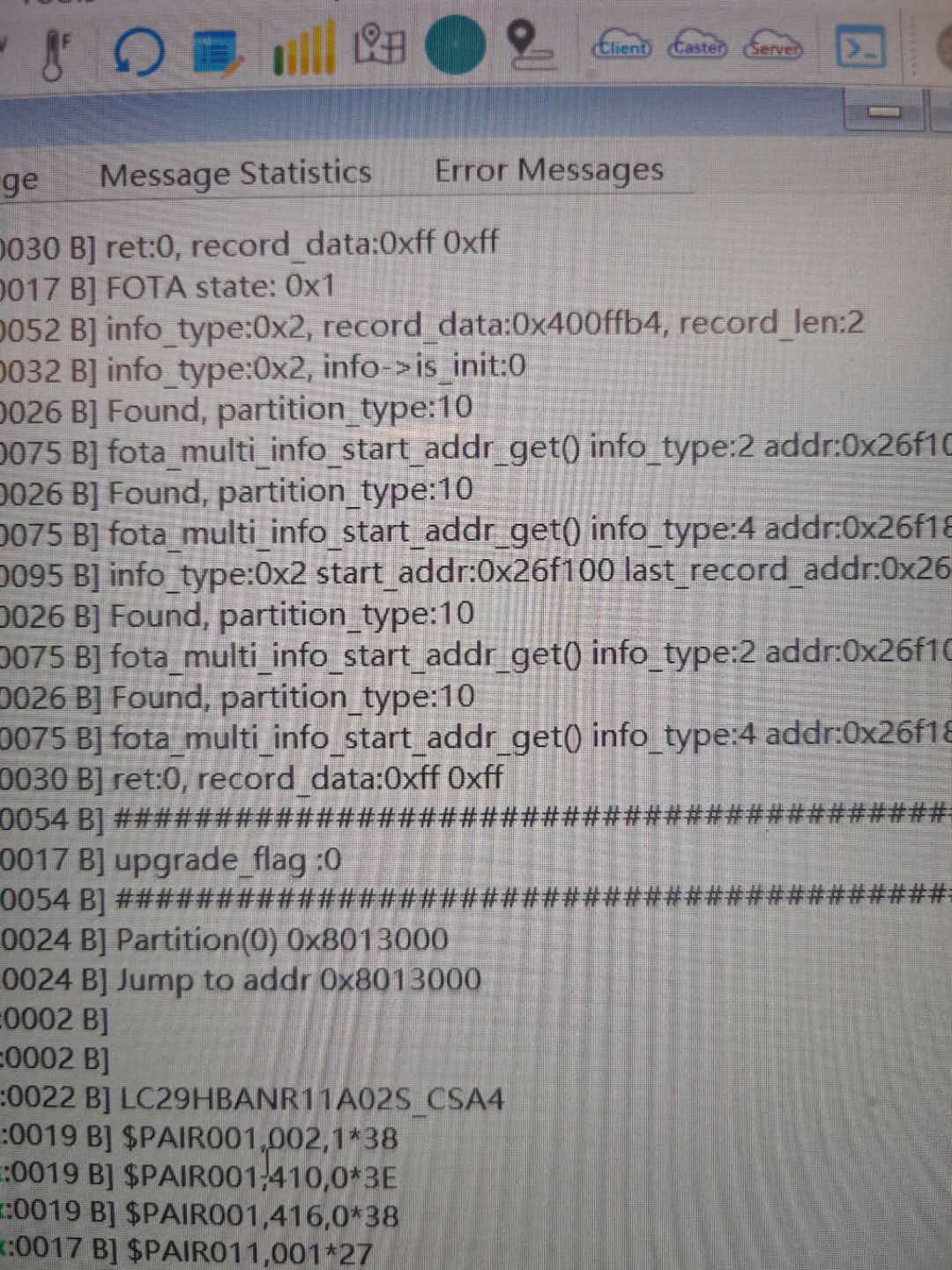
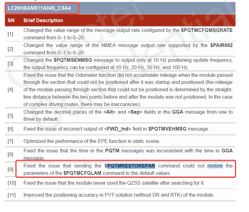
However, based on the snapshot you shared, you were using A02S_CSA4 version which is quite old. In our Firmware release Note, there was a fix for this command issue in A04S_CS4 version:

I will share you the latest FW for you to test. Take note that default baud rate is 115200 bps.

Best regards,

Hi @Jason_Siu for the latest Firmware, I have sent it to your email.

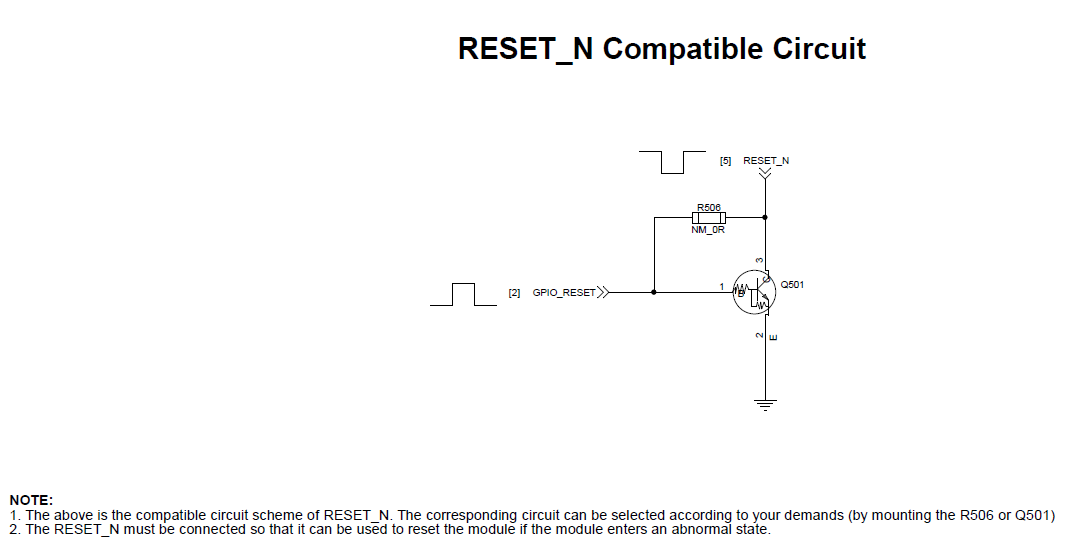
Also, can you follow below reference design? Because, when you used just the diode + resistor configuration, it was working.

For reset connection, you design was as below:

Meanwhile, the reference design circuit for RESET_N is as below:

Best regards,

Hi Mr. Firdaus,

Thank you for the clarification, this explains a lot.

I have received the FW and the latest firmware.

I’ll continue the reply in the next message, so the answer is in context.